Click here to purchase
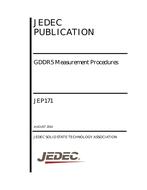
This publication is to inform all industry participants of a unified procedure to enable consistent measurement across the industry. This document contains the measurement procedures for testing GDDR5.
This document provides the test methodology details on:
- CK and WCK Timings: tCK, tWCK, tCH/tCL, tWCKH/tWCKL, CK TJ/RJrms, CK and WCK Jitter
- CK and WCK Input Operating Conditions: VIXCK, VIXWCK, VIDCK(ac), VIDWCK(ac), VIDCK(dc),VIDWCK(dc), CKslew, and WCKslew
- Data Input Timings: tDIVW, tDIPW
Note: The procedures described in this document are intended to provide information about the tests that will be used in JEDEC GDDR5 recommended measurement parameter. This testing is not a replacement for an exhaustive test validation plan.
Product Details
- Published:
- 2014
- Number of Pages:
- 34
- File Size:
- 1 file , 3 MB
